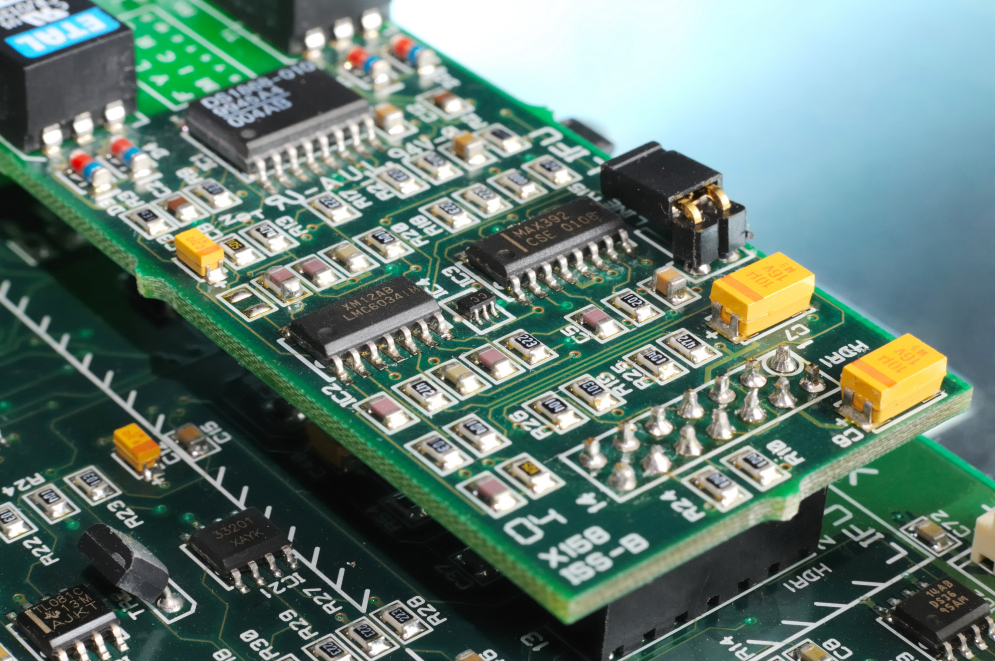
| Single Sided |
HAL, Lacquer |
| Double Sided |
HAL, TIN , Electroplated Gold & Nickel |
| Solder Mask Finish |
PISM, Liquid Solder Mask |
| Solder Mask color |
Green, White, Black, Blue ,Red |
| Legend/Ident color |
White, Black, yellow, Green |
| Special Requirement |
Carbon Printing on Push Button , Selective Gold & Nickel plating on Connecting Tabs
|
| Minimum copper thickness |
1 Oz (35 microns) |
| Maximum copper thickness |
3 Oz (105 microns) |
| Dedicated Electrical Testing (BBT) |
Available |
| PCB Cutting options |
Routing , V groove , Punching |


